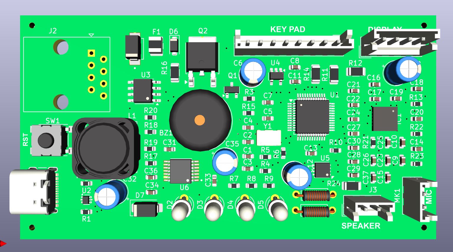
pcb design
7 min read
•2026-03-15
High-Density PCB Thermal Management and Signal Integrity for Edge IoT
Thermal dissipation modeling across 8-layer HDI stackups with buried copper microvias, impedance-matched differential pairs, and EMI shielding for sub-gigahertz transceivers.
Altium Designer 24Ansys SIwaveIPC Class 3FR408HR High-Tg
Overview & Thermal Challenge Modern high-density edge IoT gateways pack high-frequency microcontrollers, multi-protocol RF front-ends, and buck-boost power stages into ultra-compact enclosures (< 40cm³). Without rigorous thermal planning, localized thermal hotspots exceed 85°C, degrading clock jitter and introducing bit error rates in high-speed SPI/eMMC buses.
Stackup Architecture To mitigate thermal hotspots while enforcing 50Ω single-ended and 90Ω differential impedance matching, we designed an asymmetrical 8-layer stackup:
Layer 1: High-Speed Signals & RF Traces (0.5 oz Cu + ENIG)
Layer 2: Solid Ground Reference Plane (1.0 oz Cu)
Layer 3: Inner Microstrip Routing (0.5 oz Cu)
Layer 4: Continuous 3.3V / 1.8V Power Core (1.0 oz Cu)
Layer 5: Continuous Ground Plane (1.0 oz Cu)
Layer 6: Low-Frequency Control & GPIO Bus (0.5 oz Cu)
Layer 7: Ground Plane (1.0 oz Cu)
Layer 8: Thermal Sinks & Power Decoupling (1.0 oz Cu)
Thermal Via Array Analysis We implemented staggered 0.2mm mechanical microvias directly beneath the QFN power pad of the main switching regulator. Copper filling (IPC-4761 Type VII) ensured thermal conductivity jumped from 0.3 W/m·K to > 380 W/m·K through the slug array.
Signal Integrity Validations Time Domain Reflectometry (TDR) measurements confirmed differential trace impedance tolerance within ±4.2% across the full 2.4 GHz spectrum, eliminating standing wave reflections.
COLLABORATIVE R&D INQUIRY
Require Similar Hardware Architecture or Low-Power Firmware?
Schedule a confidential engineering design review with Safe Switching's Principal Hardware and Firmware Architects under mutual NDA.